Global Hearables Market to Reach $126.2B by 2032, Growing at 20.7% CAGR with AI & Health Tech Integration
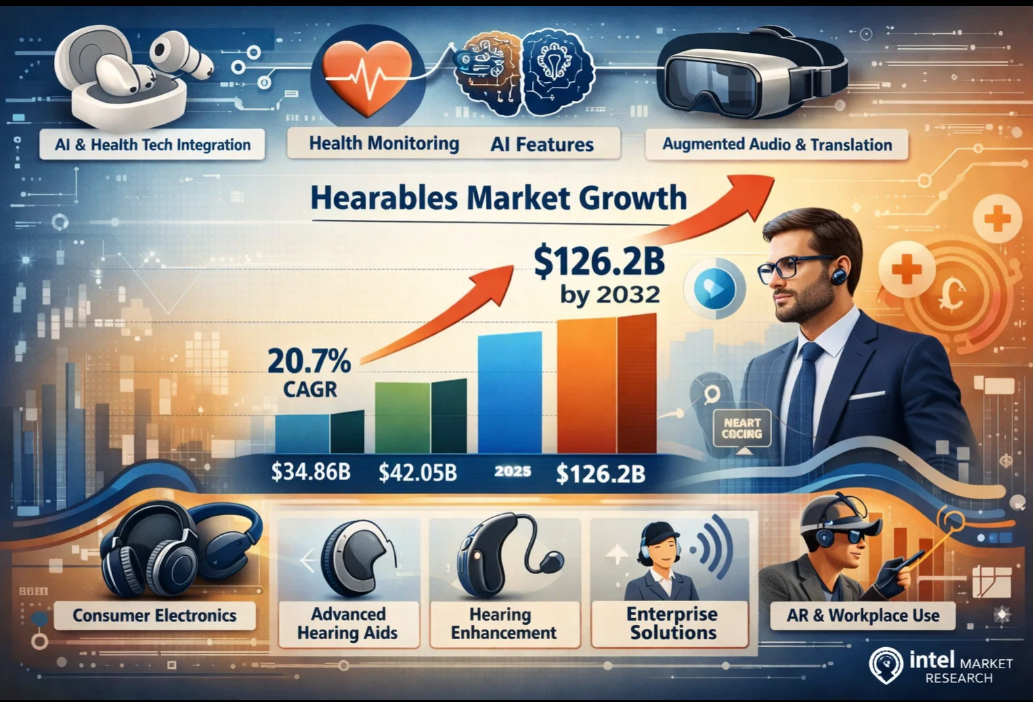
The global Hearables Market was valued at USD 34,860 million in 2024. The market is projected to grow from USD 42,050 million in 2025 to USD 126,200 million by 2032, exhibiting a CAGR of 20.7% during the forecast period. This exceptional growth trajectory is detailed in a comprehensive new report published by Intel Market Research. The study underscores how hearables are fundamentally transforming personal audio, merging high-fidelity sound with advanced connectivity and health-monitoring features.
Hearables, encompassing everything from sophisticated wireless earbuds to AI-powered hearing enhancement devices, are becoming indispensable tools for modern life. They connect us to entertainment, facilitate communication, and increasingly monitor our well-being. Their design, which prioritizes seamless integration with our digital ecosystems and daily routines, is making them a cornerstone of the connected consumer electronics landscape.
Consumer Electronics and Health & Wellness Integration: The Dual Growth Engine
The report identifies the convergence of consumer electronics with health and wellness technology as the paramount driver for hearables demand. The consumer segment, including headphones and wireless earbuds, currently holds a dominant share, fueled by the global proliferation of smartphones and the rising consumption of digital audio content. However, the healthcare segment, particularly advanced hearing aids and personal sound amplification products, is experiencing accelerated growth, driven by an aging global population and growing awareness of hearing health.
"The line between consumer entertainment devices and medical-grade hearing assistance is blurring," the report states. This is creating a new category of 'hearables' that adapt to acoustic environments, translate languages in real-time, and track vital signs like heart rate. This fusion of functionality is unlocking new user bases and applications, propelling the market forward as devices evolve from simple audio accessories to comprehensive personal assistant and health platforms.
Download FREE Sample Report:
Hearables Market - View in Detailed Research Report
Market Segmentation: Headphones & Headsets and Consumer Applications Dominate
The report provides a detailed segmentation analysis, offering a clear view of the market structure and key growth segments:
Segment Analysis:
By Type
Headphone & Headsets
Hearing Aids
By Application
Consumer
Healthcare
Others
By End User
Individual Consumers
Healthcare Institutions
Entertainment & Gaming Industry
By Technology
Bluetooth & Wireless Connectivity
Augmented Hearing & AI
Hearing Enhancement Technologies
By Distribution Channel
Online Retail
Electronics Specialty Stores
Other Retail Outlets
Get Full Report Here:
https://semiconductorinsight.com/report/hearables-market/
Competitive Landscape: Key Players and Strategic Focus
The report profiles key industry players, including:
Apple Inc.
Samsung Electronics Co., Ltd.
Sennheiser Electronic GmbH & Co. KG
Sony Corporation
GN Store Nord A/S (Jabra)
WS Audiology (Signia, Widex)
Starkey Hearing Technologies
Bose Corporation
Bragi GmbH
Valencell, Inc.
Eargo, Inc.
Harman International (AKG)
Audio-Technica Corporation
Miracle-Ear
Doppler Labs
These companies are focusing on a multi-pronged strategy. For consumer electronics giants, the focus is on creating deeper ecosystem integration, enhancing active noise cancellation, and extending battery life. For audiology-focused players, the strategy revolves around incorporating consumer-friendly designs with clinically validated hearing enhancement, making their products more accessible and less stigmatized. Across the board, investment in AI for personalized audio experiences and health sensing is a universal priority to create differentiated value propositions.
Emerging Opportunities in Enterprise and Augmented Audio
Beyond the core consumer market, the report outlines significant emerging opportunities. The enterprise sector is a major new frontier, with hearables being adopted for unified communications, enabling hands-free operation in logistics and manufacturing, and providing real-time language translation for global teams. Furthermore, the integration of Augmented Reality audio is a major trend, creating immersive experiences for gaming, navigation, and interactive learning. Hearables with embedded biometric sensors are also moving beyond fitness tracking into mainstream health monitoring, offering potential for early detection of conditions based on auditory and physiological data.
Report Scope and Availability
The market research report offers a comprehensive analysis of the global and regional Hearables markets from 2025–2032. It provides detailed segmentation, market size forecasts, competitive intelligence, technology trends, and an evaluation of key market dynamics.
For a detailed analysis of market drivers, restraints, opportunities, and the competitive strategies of key players, access the complete report.
About Intel Market Research
Intel Market Research is a leading provider of market intelligence and strategic consulting for global technology and consumer electronics industries. Our in-depth reports and analysis offer actionable insights to help businesses navigate complex market dynamics, identify growth opportunities, and make informed decisions. We are committed to delivering high-quality, data-driven research to our clients worldwide.
Website: https://www.intelmarketresearch.com/
International: +1 888 328 2189
LinkedIn: Follow Us
#HearablesMarket #WirelessEarbuds #SmartHeadphones #AudioTechnology #ConsumerElectronics #HearingAids #HealthTech #AIInAudio #WearableTechnology #BluetoothDevices #ARAudio #DigitalHealth #TechInnovation #MarketResearch #ConsumerTech
Global Hearables Market to Reach $126.2B by 2032, Growing at 20.7% CAGR with AI & Health Tech Integration
The global Hearables Market was valued at USD 34,860 million in 2024. The market is projected to grow from USD 42,050 million in 2025 to USD 126,200 million by 2032, exhibiting a CAGR of 20.7% during the forecast period. This exceptional growth trajectory is detailed in a comprehensive new report published by Intel Market Research. The study underscores how hearables are fundamentally transforming personal audio, merging high-fidelity sound with advanced connectivity and health-monitoring features.
Hearables, encompassing everything from sophisticated wireless earbuds to AI-powered hearing enhancement devices, are becoming indispensable tools for modern life. They connect us to entertainment, facilitate communication, and increasingly monitor our well-being. Their design, which prioritizes seamless integration with our digital ecosystems and daily routines, is making them a cornerstone of the connected consumer electronics landscape.
Consumer Electronics and Health & Wellness Integration: The Dual Growth Engine
The report identifies the convergence of consumer electronics with health and wellness technology as the paramount driver for hearables demand. The consumer segment, including headphones and wireless earbuds, currently holds a dominant share, fueled by the global proliferation of smartphones and the rising consumption of digital audio content. However, the healthcare segment, particularly advanced hearing aids and personal sound amplification products, is experiencing accelerated growth, driven by an aging global population and growing awareness of hearing health.
"The line between consumer entertainment devices and medical-grade hearing assistance is blurring," the report states. This is creating a new category of 'hearables' that adapt to acoustic environments, translate languages in real-time, and track vital signs like heart rate. This fusion of functionality is unlocking new user bases and applications, propelling the market forward as devices evolve from simple audio accessories to comprehensive personal assistant and health platforms.
Download FREE Sample Report:
Hearables Market - View in Detailed Research Report
Market Segmentation: Headphones & Headsets and Consumer Applications Dominate
The report provides a detailed segmentation analysis, offering a clear view of the market structure and key growth segments:
Segment Analysis:
By Type
Headphone & Headsets
Hearing Aids
By Application
Consumer
Healthcare
Others
By End User
Individual Consumers
Healthcare Institutions
Entertainment & Gaming Industry
By Technology
Bluetooth & Wireless Connectivity
Augmented Hearing & AI
Hearing Enhancement Technologies
By Distribution Channel
Online Retail
Electronics Specialty Stores
Other Retail Outlets
Get Full Report Here:
https://semiconductorinsight.com/report/hearables-market/
Competitive Landscape: Key Players and Strategic Focus
The report profiles key industry players, including:
Apple Inc.
Samsung Electronics Co., Ltd.
Sennheiser Electronic GmbH & Co. KG
Sony Corporation
GN Store Nord A/S (Jabra)
WS Audiology (Signia, Widex)
Starkey Hearing Technologies
Bose Corporation
Bragi GmbH
Valencell, Inc.
Eargo, Inc.
Harman International (AKG)
Audio-Technica Corporation
Miracle-Ear
Doppler Labs
These companies are focusing on a multi-pronged strategy. For consumer electronics giants, the focus is on creating deeper ecosystem integration, enhancing active noise cancellation, and extending battery life. For audiology-focused players, the strategy revolves around incorporating consumer-friendly designs with clinically validated hearing enhancement, making their products more accessible and less stigmatized. Across the board, investment in AI for personalized audio experiences and health sensing is a universal priority to create differentiated value propositions.
Emerging Opportunities in Enterprise and Augmented Audio
Beyond the core consumer market, the report outlines significant emerging opportunities. The enterprise sector is a major new frontier, with hearables being adopted for unified communications, enabling hands-free operation in logistics and manufacturing, and providing real-time language translation for global teams. Furthermore, the integration of Augmented Reality audio is a major trend, creating immersive experiences for gaming, navigation, and interactive learning. Hearables with embedded biometric sensors are also moving beyond fitness tracking into mainstream health monitoring, offering potential for early detection of conditions based on auditory and physiological data.
Report Scope and Availability
The market research report offers a comprehensive analysis of the global and regional Hearables markets from 2025–2032. It provides detailed segmentation, market size forecasts, competitive intelligence, technology trends, and an evaluation of key market dynamics.
For a detailed analysis of market drivers, restraints, opportunities, and the competitive strategies of key players, access the complete report.
About Intel Market Research
Intel Market Research is a leading provider of market intelligence and strategic consulting for global technology and consumer electronics industries. Our in-depth reports and analysis offer actionable insights to help businesses navigate complex market dynamics, identify growth opportunities, and make informed decisions. We are committed to delivering high-quality, data-driven research to our clients worldwide.
🌐 Website: https://www.intelmarketresearch.com/
📞 International: +1 888 328 2189
🔗 LinkedIn: Follow Us
#HearablesMarket #WirelessEarbuds #SmartHeadphones #AudioTechnology #ConsumerElectronics #HearingAids #HealthTech #AIInAudio #WearableTechnology #BluetoothDevices #ARAudio #DigitalHealth #TechInnovation #MarketResearch #ConsumerTech
0 Yorumlar
0 hisse senetleri
38 Views
0 önizleme