Wireless Power Supply for Semiconductor Market to Reach $126M by 2032 | 8.1% CAGR Growth Report
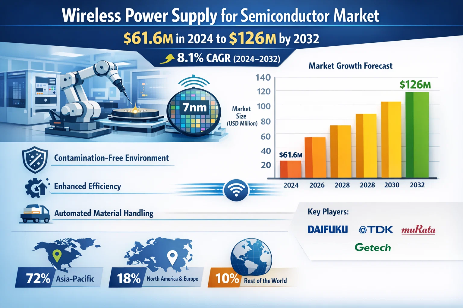
The global Wireless Power Supply (WPS) for Semiconductor Market, valued at USD 61.6 million in 2024, is poised for substantial expansion, projected to reach USD 126 million by 2032 with a compound annual growth rate (CAGR) of 8.1%. This growth trajectory is detailed in a comprehensive new report published by Semiconductor Insight, highlighting the critical role of wireless power solutions in enabling advanced semiconductor manufacturing processes while improving operational efficiency.
Wireless power supply systems have become indispensable in semiconductor fabrication facilities where contamination-free environments are paramount. By eliminating physical connectors, WPS technology significantly reduces particle generation - a crucial advantage when dealing with nanometer-scale semiconductor manufacturing where a single speck of dust can ruin an entire wafer. The inherent flexibility of wireless systems also enables seamless integration with automated material handling equipment, translating to measurable improvements in production line uptime.
Download FREE Sample Report:
Wireless Power Supply (WPS) for Semiconductor Market - View in Detailed Research Report
Semiconductor Manufacturing Evolution Drives WPS Adoption
The report identifies rapid advancements in semiconductor manufacturing technology as the primary catalyst for WPS market growth. As chipmakers transition to more advanced process nodes below 7nm, the need for ultra-clean manufacturing environments has become non-negotiable. Wireless power eliminates one of the last remaining sources of particulate contamination in cleanrooms - the physical connectors required for traditional power transmission.
"What we're seeing is a fundamental shift in semiconductor fab design philosophy," explains the report. "Leading-edge fabs in Taiwan and South Korea are now specifying wireless power as standard for all mobile equipment, recognizing that the contamination reduction benefits outweigh the incremental cost." The report notes that these two countries alone account for nearly 65% of global WPS deployments in semiconductor applications, reflecting their dominance in advanced chip manufacturing.
Market Segmentation Reveals Key Growth Areas
The report provides detailed segmentation of the WPS for Semiconductor Market, identifying the most promising opportunities:
Segment Analysis:
By Component
Transmitter Units
Receiver Units
Control Systems
Ancillary Components
By Power Output
Low Power (<1kW)
Medium Power (1-10kW)
High Power (>10kW)
By Wafer Size
200mm Wafer Applications
300mm Wafer Applications
Emerging 450mm Compatibility
Technology Innovation Unlocks New Possibilities
Recent breakthroughs in resonant inductive coupling technology have addressed many of the efficiency challenges that previously limited WPS adoption in semiconductor applications. Modern systems now achieve power transfer efficiencies exceeding 90% even at the higher power levels required for wafer handling robots and other fab equipment. Temperature sensitivity has also improved dramatically, with some systems maintaining stable operation across the full range of temperatures encountered in semiconductor processing environments.
The integration of Industry 4.0 capabilities is creating additional value. Smart WPS systems can now provide real-time performance data and predictive maintenance alerts, further enhancing equipment uptime. Some advanced implementations even incorporate dynamic power adjustment features that optimize energy usage based on the operational state of connected equipment.
Competitive Landscape: Technology Leaders Drive Innovation
The report profiles the key players shaping the WPS for Semiconductor Market:
Daifuku (Japan)
TDK Corporation (Japan)
Murata Machinery (Japan)
Omron Corporation (Japan)
Panasonic Corporation (Japan)
Yaskawa Electric Corporation (Japan)
Mitsubishi Electric (Japan)
IHI Corporation (Japan)
Jiangsu Tota Intelligent Technology (China)
Getech Technology (China)
Wiferion (Germany)
B&PLUS (Japan)
Japanese companies maintain technological leadership in this space, leveraging decades of experience in industrial automation and precision manufacturing. However, the report notes increasing competition from Chinese manufacturers offering cost-effective alternatives for less demanding applications. European and American players are focusing on niche applications requiring the highest levels of precision and reliability.
Regional Dynamics Reflect Semiconductor Manufacturing Concentrations
Geographically, the Asia-Pacific region dominates the WPS for Semiconductor Market, accounting for over 72% of global demand. This concentration directly mirrors the region's status as the world's semiconductor manufacturing hub. Within Asia, Taiwan, South Korea, and Japan represent the most advanced markets, with China showing the fastest growth rate as its domestic semiconductor industry expands rapidly.
North America and Europe maintain significant positions in the market, particularly for research and development applications and specialized manufacturing processes. These regions benefit from strong technology ecosystems and early adoption of innovative solutions. The Middle East and Latin America are emerging as growth markets, though from smaller bases, as global semiconductor manufacturers diversify their production footprints.
Future Outlook: Wireless Power as Standard Fab Infrastructure
Looking ahead, the report predicts wireless power will become standard infrastructure in new semiconductor fabs, much like ultra-pure water and specialty gas systems are today. The technology's ability to support higher power applications continues to improve, opening up new use cases in semiconductor manufacturing beyond material handling.
Emerging applications such as wireless-powered process chamber components and mobile metrology equipment are already in development. The coming years will likely see wireless power become deeply embedded throughout the semiconductor manufacturing workflow, from wafer fabrication through final testing and packaging.
Get Full Report Here:
https://semiconductorinsight.com/report/wireless-power-supply-wps-for-semiconductor-market/
Report Scope and Availability
The market research report provides a comprehensive analysis of the global and regional WPS for Semiconductor markets from 2024–2032. It includes detailed segmentation, market size forecasts, competitive intelligence, technology trends, and an evaluation of key market dynamics.
Download FREE Sample Report:
Wireless Power Supply (WPS) for Semiconductor Market - View in Detailed Research Report
About Semiconductor Insight
Semiconductor Insight is a leading provider of market intelligence and strategic consulting for the global semiconductor and high-technology industries. Our in-depth reports and analysis offer actionable insights to help businesses navigate complex market dynamics, identify growth opportunities, and make informed decisions. We are committed to delivering high-quality, data-driven research to our clients worldwide.
Website:
https://semiconductorinsight.com/
International: +91 8087 99 2013
LinkedIn: Follow Us
#WirelessPower #SemiconductorMarket
#WirelessPowerSupply #SemiconductorIndustry #ChipManufacturing #CleanroomTechnology #Industry40 #SemiconductorTechnology #MarketGrowth
#PowerTransfer #AutomationTechnology #ElectronicsIndustry #TechInnovation #SemiconductorTrends #FutureOfSemiconductors
Wireless Power Supply for Semiconductor Market to Reach $126M by 2032 | 8.1% CAGR Growth Report
The global Wireless Power Supply (WPS) for Semiconductor Market, valued at USD 61.6 million in 2024, is poised for substantial expansion, projected to reach USD 126 million by 2032 with a compound annual growth rate (CAGR) of 8.1%. This growth trajectory is detailed in a comprehensive new report published by Semiconductor Insight, highlighting the critical role of wireless power solutions in enabling advanced semiconductor manufacturing processes while improving operational efficiency.
Wireless power supply systems have become indispensable in semiconductor fabrication facilities where contamination-free environments are paramount. By eliminating physical connectors, WPS technology significantly reduces particle generation - a crucial advantage when dealing with nanometer-scale semiconductor manufacturing where a single speck of dust can ruin an entire wafer. The inherent flexibility of wireless systems also enables seamless integration with automated material handling equipment, translating to measurable improvements in production line uptime.
Download FREE Sample Report:
Wireless Power Supply (WPS) for Semiconductor Market - View in Detailed Research Report
Semiconductor Manufacturing Evolution Drives WPS Adoption
The report identifies rapid advancements in semiconductor manufacturing technology as the primary catalyst for WPS market growth. As chipmakers transition to more advanced process nodes below 7nm, the need for ultra-clean manufacturing environments has become non-negotiable. Wireless power eliminates one of the last remaining sources of particulate contamination in cleanrooms - the physical connectors required for traditional power transmission.
"What we're seeing is a fundamental shift in semiconductor fab design philosophy," explains the report. "Leading-edge fabs in Taiwan and South Korea are now specifying wireless power as standard for all mobile equipment, recognizing that the contamination reduction benefits outweigh the incremental cost." The report notes that these two countries alone account for nearly 65% of global WPS deployments in semiconductor applications, reflecting their dominance in advanced chip manufacturing.
Market Segmentation Reveals Key Growth Areas
The report provides detailed segmentation of the WPS for Semiconductor Market, identifying the most promising opportunities:
Segment Analysis:
By Component
Transmitter Units
Receiver Units
Control Systems
Ancillary Components
By Power Output
Low Power (<1kW)
Medium Power (1-10kW)
High Power (>10kW)
By Wafer Size
200mm Wafer Applications
300mm Wafer Applications
Emerging 450mm Compatibility
Technology Innovation Unlocks New Possibilities
Recent breakthroughs in resonant inductive coupling technology have addressed many of the efficiency challenges that previously limited WPS adoption in semiconductor applications. Modern systems now achieve power transfer efficiencies exceeding 90% even at the higher power levels required for wafer handling robots and other fab equipment. Temperature sensitivity has also improved dramatically, with some systems maintaining stable operation across the full range of temperatures encountered in semiconductor processing environments.
The integration of Industry 4.0 capabilities is creating additional value. Smart WPS systems can now provide real-time performance data and predictive maintenance alerts, further enhancing equipment uptime. Some advanced implementations even incorporate dynamic power adjustment features that optimize energy usage based on the operational state of connected equipment.
Competitive Landscape: Technology Leaders Drive Innovation
The report profiles the key players shaping the WPS for Semiconductor Market:
Daifuku (Japan)
TDK Corporation (Japan)
Murata Machinery (Japan)
Omron Corporation (Japan)
Panasonic Corporation (Japan)
Yaskawa Electric Corporation (Japan)
Mitsubishi Electric (Japan)
IHI Corporation (Japan)
Jiangsu Tota Intelligent Technology (China)
Getech Technology (China)
Wiferion (Germany)
B&PLUS (Japan)
Japanese companies maintain technological leadership in this space, leveraging decades of experience in industrial automation and precision manufacturing. However, the report notes increasing competition from Chinese manufacturers offering cost-effective alternatives for less demanding applications. European and American players are focusing on niche applications requiring the highest levels of precision and reliability.
Regional Dynamics Reflect Semiconductor Manufacturing Concentrations
Geographically, the Asia-Pacific region dominates the WPS for Semiconductor Market, accounting for over 72% of global demand. This concentration directly mirrors the region's status as the world's semiconductor manufacturing hub. Within Asia, Taiwan, South Korea, and Japan represent the most advanced markets, with China showing the fastest growth rate as its domestic semiconductor industry expands rapidly.
North America and Europe maintain significant positions in the market, particularly for research and development applications and specialized manufacturing processes. These regions benefit from strong technology ecosystems and early adoption of innovative solutions. The Middle East and Latin America are emerging as growth markets, though from smaller bases, as global semiconductor manufacturers diversify their production footprints.
Future Outlook: Wireless Power as Standard Fab Infrastructure
Looking ahead, the report predicts wireless power will become standard infrastructure in new semiconductor fabs, much like ultra-pure water and specialty gas systems are today. The technology's ability to support higher power applications continues to improve, opening up new use cases in semiconductor manufacturing beyond material handling.
Emerging applications such as wireless-powered process chamber components and mobile metrology equipment are already in development. The coming years will likely see wireless power become deeply embedded throughout the semiconductor manufacturing workflow, from wafer fabrication through final testing and packaging.
Get Full Report Here:
https://semiconductorinsight.com/report/wireless-power-supply-wps-for-semiconductor-market/
Report Scope and Availability
The market research report provides a comprehensive analysis of the global and regional WPS for Semiconductor markets from 2024–2032. It includes detailed segmentation, market size forecasts, competitive intelligence, technology trends, and an evaluation of key market dynamics.
Download FREE Sample Report:
Wireless Power Supply (WPS) for Semiconductor Market - View in Detailed Research Report
About Semiconductor Insight
Semiconductor Insight is a leading provider of market intelligence and strategic consulting for the global semiconductor and high-technology industries. Our in-depth reports and analysis offer actionable insights to help businesses navigate complex market dynamics, identify growth opportunities, and make informed decisions. We are committed to delivering high-quality, data-driven research to our clients worldwide.
🌐 Website: https://semiconductorinsight.com/
📞 International: +91 8087 99 2013
🔗 LinkedIn: Follow Us
#WirelessPower #SemiconductorMarket
#WirelessPowerSupply #SemiconductorIndustry #ChipManufacturing #CleanroomTechnology #Industry40 #SemiconductorTechnology #MarketGrowth
#PowerTransfer #AutomationTechnology #ElectronicsIndustry #TechInnovation #SemiconductorTrends #FutureOfSemiconductors