APD Avalanche Photodiode Market to Reach USD 179 Million by 2032 Driven by Automotive LiDAR and Optical Communication Growth
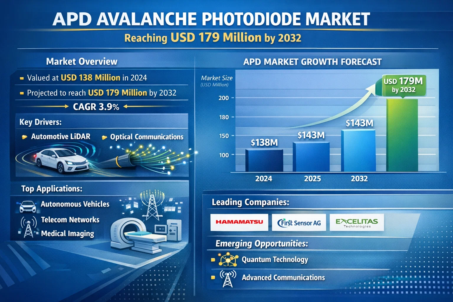
The global APD Avalanche Photodiode Market was valued at USD 138 million in 2024. The market is projected to grow from USD 143 million in 2025 to USD 179 million by 2032, exhibiting a CAGR of 3.9% during the forecast period, according to a comprehensive new report published by Semiconductor Insight. This growth trajectory highlights the expanding role of APDs as critical components in systems requiring highly sensitive light detection, particularly in fields like autonomous driving, telecommunications, and medical imaging.
Avalanche Photodiodes (APDs) are semiconductor devices that leverage the avalanche multiplication effect to detect low-intensity light signals with exceptional sensitivity and speed. This unique capability makes them indispensable in applications where traditional photodetectors fall short, such as long-range LiDAR, high-speed optical communication networks, and precision medical diagnostics. Their function in converting light into electrical signals with internal gain allows systems to operate effectively even in challenging low-light conditions, positioning APDs as foundational technology for numerous advanced systems.
Download FREE Sample Report:
APD Avalanche Photodiode Market - View in Detailed Research Report
Automotive and LiDAR Expansion: The Primary Growth Engine
The report identifies the rapid advancement and adoption of Automotive LiDAR as the paramount driver for the APD market's growth. The proliferation of autonomous vehicles and advanced driver-assistance systems (ADAS) is creating robust demand for high-sensitivity LiDAR systems that rely on APDs for accurate object detection and ranging. This segment's demand is propelled by the rapid integration of LiDAR technology into next-generation vehicles for enhanced autonomy and safety features. High-volume production requirements and stringent quality standards from automotive companies drive innovation and economies of scale in APD manufacturing.
"The strategic focus on developing next-generation LiDAR systems for automotive safety and smart manufacturing applications continues to propel the demand for high-performance avalanche photodiodes," the report states. Collaborations between APD suppliers and automotive leaders are crucial for developing customized solutions that meet the demanding performance and reliability specifications of the automotive industry. The transition towards higher levels of vehicle autonomy, which requires more sophisticated and reliable sensing capabilities, further intensifies this trend.
Read Full Report:
https://semiconductorinsight.com/report/apd-avalanche-photodiode-market/
Market Segmentation: Si APD and Automotive Applications Driving Dominance
The report provides a detailed segmentation analysis, offering a clear view of the market structure and key growth segments:
Segment Analysis:
By Type
Si APD
InGaAs APD
Others
By Application
Industrial
Medical
Mobility
Others
By End User
Automotive OEMs & Tier-1 Suppliers
Telecommunication Service Providers
Medical Device Manufacturers
Industrial Equipment Manufacturers
Download Sample Report:
https://semiconductorinsight.com/download-sample-report/?product_id=127114
Competitive Landscape: Key Players and Strategic Focus
The global APD Avalanche Photodiode market is moderately concentrated, with the top three manufacturers collectively holding over 45% of the market share. Hamamatsu Photonics K.K. and First Sensor AG are recognized as global leaders, leveraging their extensive R&D capabilities and established semiconductor manufacturing expertise to dominate the high-performance segment. Their products are critical in applications requiring extreme sensitivity, such as LiDAR for autonomous vehicles and high-speed optical communication systems.
The report profiles key industry players, including:
Hamamatsu Photonics K.K. (Japan)
First Sensor AG (Germany)
Kyosemi Corporation (Japan)
Luna Optoelectronics (U.S.)
Excelitas Technologies Corp. (U.S.)
Edmund Optics (U.S.)
GCS (China)
Accelink Technologies Co., Ltd. (China)
NORINCO GROUP (China)
LD-PD Inc. (U.S.)
Voxtel, Inc. (U.S.)
Laser Components GmbH (Germany)
Albis Optoelectronics AG (Switzerland)
These companies are intensely focused on technological differentiation and material science innovation to enhance performance metrics such as quantum efficiency and noise characteristics. Many are also pursuing geographic expansion into high-growth regions to capture emerging opportunities, particularly in the Asia-Pacific market where manufacturing capabilities are rapidly scaling.
Emerging Opportunities in Quantum Technology and Advanced Communications
While automotive LiDAR represents the current growth frontier, the report outlines significant emerging opportunities in quantum technology and next-generation communications. The development of quantum computing and quantum key distribution (QKD) systems requires photodetectors with single-photon sensitivity, a domain where specialized APDs excel. Furthermore, the ongoing global expansion of fiber-optic communication infrastructure, including the push for higher bandwidth 5G and eventual 6G networks, creates sustained demand for high-speed APDs in optical receivers. The integration of APDs into new industrial automation and safety systems further expands their application horizon, underscoring their versatility beyond traditional markets.
Report Scope and Availability
The market research report offers a comprehensive analysis of the global and regional APD Avalanche Photodiode markets from 2025-2032. It provides detailed segmentation, market size forecasts, competitive intelligence, technology trends, and an evaluation of key market dynamics, including the impact of material innovations like InGaAs for longer wavelength detection and the competitive pressures shaping the industry landscape.
For a detailed analysis of market drivers, restraints, opportunities, and the competitive strategies of key players, access the complete report.
Get Full Report Here: APD Avalanche Photodiode Market, Global Business Strategies 2025-2032 - View in Detailed Research Report
Download Sample Report:
https://semiconductorinsight.com/download-sample-report/?product_id=127114
About Semiconductor Insight
Semiconductor Insight is a leading provider of market intelligence and strategic consulting for the global semiconductor and high-technology industries. Our in-depth reports and analysis offer actionable insights to help businesses navigate complex market dynamics, identify growth opportunities, and make informed decisions. We are committed to delivering high-quality, data-driven research to our clients worldwide.
🌐 Website:
https://semiconductorinsight.com/
📞 International: +91 8087 99 2013
🔗 LinkedIn: Follow Us
#APDMarket
#AvalanchePhotodiode
#SemiconductorIndustry
#LiDARTechnology
#AutonomousVehicles
#OpticalCommunication
#Photonics
#QuantumTechnology
#ADAS
#Optoelectronics
#SemiconductorMarket
#TechInnovation
APD Avalanche Photodiode Market to Reach USD 179 Million by 2032 Driven by Automotive LiDAR and Optical Communication Growth
The global APD Avalanche Photodiode Market was valued at USD 138 million in 2024. The market is projected to grow from USD 143 million in 2025 to USD 179 million by 2032, exhibiting a CAGR of 3.9% during the forecast period, according to a comprehensive new report published by Semiconductor Insight. This growth trajectory highlights the expanding role of APDs as critical components in systems requiring highly sensitive light detection, particularly in fields like autonomous driving, telecommunications, and medical imaging.
Avalanche Photodiodes (APDs) are semiconductor devices that leverage the avalanche multiplication effect to detect low-intensity light signals with exceptional sensitivity and speed. This unique capability makes them indispensable in applications where traditional photodetectors fall short, such as long-range LiDAR, high-speed optical communication networks, and precision medical diagnostics. Their function in converting light into electrical signals with internal gain allows systems to operate effectively even in challenging low-light conditions, positioning APDs as foundational technology for numerous advanced systems.
Download FREE Sample Report:
APD Avalanche Photodiode Market - View in Detailed Research Report
Automotive and LiDAR Expansion: The Primary Growth Engine
The report identifies the rapid advancement and adoption of Automotive LiDAR as the paramount driver for the APD market's growth. The proliferation of autonomous vehicles and advanced driver-assistance systems (ADAS) is creating robust demand for high-sensitivity LiDAR systems that rely on APDs for accurate object detection and ranging. This segment's demand is propelled by the rapid integration of LiDAR technology into next-generation vehicles for enhanced autonomy and safety features. High-volume production requirements and stringent quality standards from automotive companies drive innovation and economies of scale in APD manufacturing.
"The strategic focus on developing next-generation LiDAR systems for automotive safety and smart manufacturing applications continues to propel the demand for high-performance avalanche photodiodes," the report states. Collaborations between APD suppliers and automotive leaders are crucial for developing customized solutions that meet the demanding performance and reliability specifications of the automotive industry. The transition towards higher levels of vehicle autonomy, which requires more sophisticated and reliable sensing capabilities, further intensifies this trend.
Read Full Report: https://semiconductorinsight.com/report/apd-avalanche-photodiode-market/
Market Segmentation: Si APD and Automotive Applications Driving Dominance
The report provides a detailed segmentation analysis, offering a clear view of the market structure and key growth segments:
Segment Analysis:
By Type
Si APD
InGaAs APD
Others
By Application
Industrial
Medical
Mobility
Others
By End User
Automotive OEMs & Tier-1 Suppliers
Telecommunication Service Providers
Medical Device Manufacturers
Industrial Equipment Manufacturers
Download Sample Report: https://semiconductorinsight.com/download-sample-report/?product_id=127114
Competitive Landscape: Key Players and Strategic Focus
The global APD Avalanche Photodiode market is moderately concentrated, with the top three manufacturers collectively holding over 45% of the market share. Hamamatsu Photonics K.K. and First Sensor AG are recognized as global leaders, leveraging their extensive R&D capabilities and established semiconductor manufacturing expertise to dominate the high-performance segment. Their products are critical in applications requiring extreme sensitivity, such as LiDAR for autonomous vehicles and high-speed optical communication systems.
The report profiles key industry players, including:
Hamamatsu Photonics K.K. (Japan)
First Sensor AG (Germany)
Kyosemi Corporation (Japan)
Luna Optoelectronics (U.S.)
Excelitas Technologies Corp. (U.S.)
Edmund Optics (U.S.)
GCS (China)
Accelink Technologies Co., Ltd. (China)
NORINCO GROUP (China)
LD-PD Inc. (U.S.)
Voxtel, Inc. (U.S.)
Laser Components GmbH (Germany)
Albis Optoelectronics AG (Switzerland)
These companies are intensely focused on technological differentiation and material science innovation to enhance performance metrics such as quantum efficiency and noise characteristics. Many are also pursuing geographic expansion into high-growth regions to capture emerging opportunities, particularly in the Asia-Pacific market where manufacturing capabilities are rapidly scaling.
Emerging Opportunities in Quantum Technology and Advanced Communications
While automotive LiDAR represents the current growth frontier, the report outlines significant emerging opportunities in quantum technology and next-generation communications. The development of quantum computing and quantum key distribution (QKD) systems requires photodetectors with single-photon sensitivity, a domain where specialized APDs excel. Furthermore, the ongoing global expansion of fiber-optic communication infrastructure, including the push for higher bandwidth 5G and eventual 6G networks, creates sustained demand for high-speed APDs in optical receivers. The integration of APDs into new industrial automation and safety systems further expands their application horizon, underscoring their versatility beyond traditional markets.
Report Scope and Availability
The market research report offers a comprehensive analysis of the global and regional APD Avalanche Photodiode markets from 2025-2032. It provides detailed segmentation, market size forecasts, competitive intelligence, technology trends, and an evaluation of key market dynamics, including the impact of material innovations like InGaAs for longer wavelength detection and the competitive pressures shaping the industry landscape.
For a detailed analysis of market drivers, restraints, opportunities, and the competitive strategies of key players, access the complete report.
Get Full Report Here: APD Avalanche Photodiode Market, Global Business Strategies 2025-2032 - View in Detailed Research Report
Download Sample Report: https://semiconductorinsight.com/download-sample-report/?product_id=127114
About Semiconductor Insight
Semiconductor Insight is a leading provider of market intelligence and strategic consulting for the global semiconductor and high-technology industries. Our in-depth reports and analysis offer actionable insights to help businesses navigate complex market dynamics, identify growth opportunities, and make informed decisions. We are committed to delivering high-quality, data-driven research to our clients worldwide.
🌐 Website: https://semiconductorinsight.com/
📞 International: +91 8087 99 2013
🔗 LinkedIn: Follow Us
#APDMarket
#AvalanchePhotodiode
#SemiconductorIndustry
#LiDARTechnology
#AutonomousVehicles
#OpticalCommunication
#Photonics
#QuantumTechnology
#ADAS
#Optoelectronics
#SemiconductorMarket
#TechInnovation