Global PhotoMOS Relays Market Growth to 2034 at 5.1% CAGR Driven by Automation & EV Demand
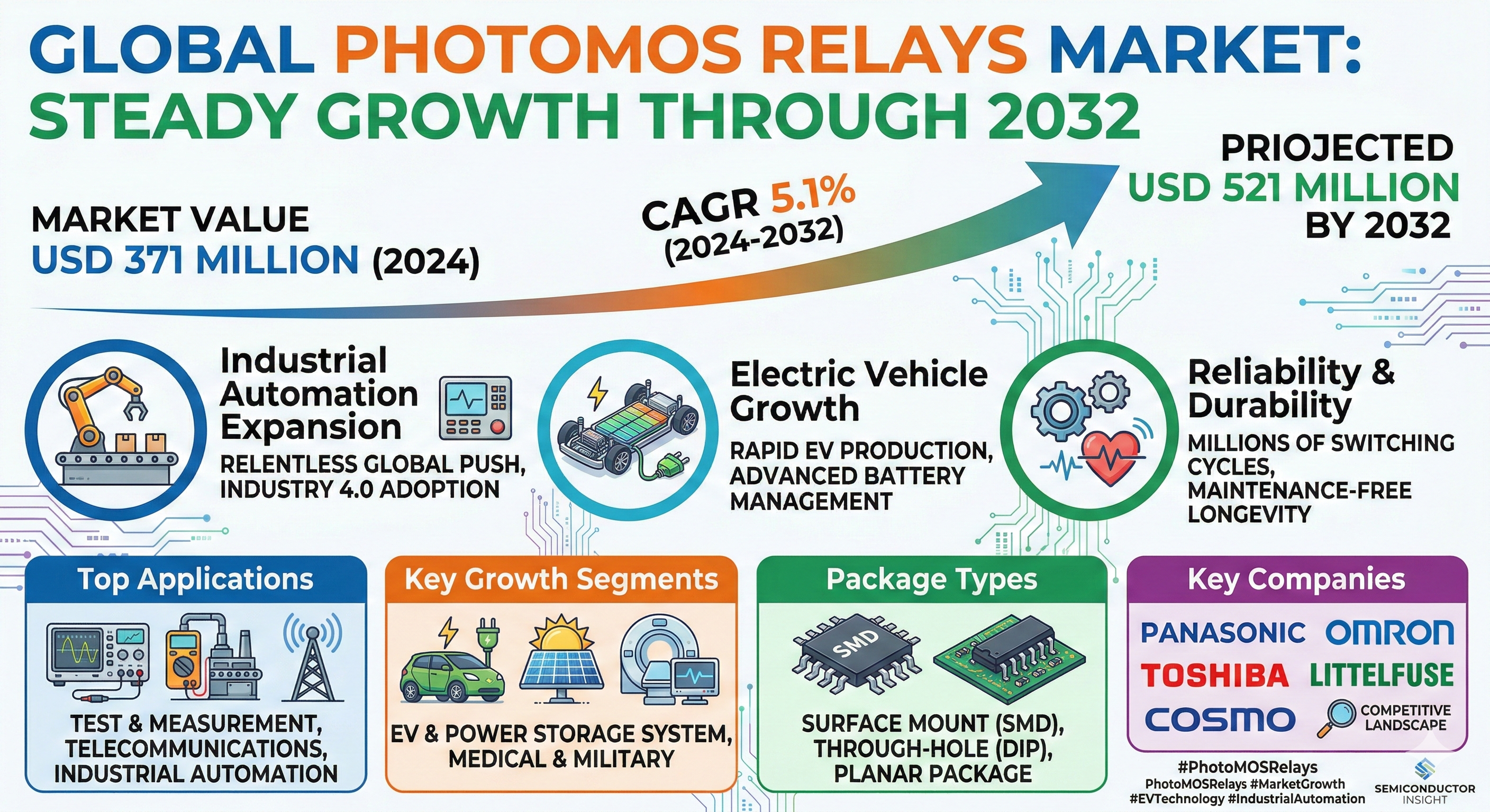
Global PhotoMOS Relays Market is on a steady growth trajectory, with its value projected to increase from USD 371 million in 2024 to USD 521 million by 2032, achieving a steady compound annual growth rate (CAGR) of 5.1% according to a comprehensive new report by Semiconductor Insight. This solid-state switching component, which uses an LED and a photo-sensitive semiconductor to achieve electrical isolation, is becoming indispensable across numerous high-reliability applications. Its unique characteristics enable silent, bounce-free, and long-lasting operation, making it a cornerstone of modern electronic control systems where precision and durability are paramount.
PhotoMOS relays, essential for providing robust isolation and reliable signal switching, are experiencing widespread adoption as industries prioritize operational efficiency and equipment longevity. Their ability to withstand millions of switching cycles without degradation makes them the preferred choice over traditional electromechanical relays in scenarios demanding maintenance-free longevity and high-speed operation. This fundamental performance advantage is driving their integration into critical infrastructure, from automated production lines to advanced telecommunications networks, where failure is not an option. Download FREE Sample Report:
PhotoMOS Relays Market - View in Detailed Research Report
Industrial Automation Expansion: The Primary Market Driver
The report identifies the relentless global push towards industrial automation as the paramount driver for PhotoMOS relay demand. This trend is largely fueled by the global adoption of Industry 4.0 principles and the ongoing need to optimize manufacturing processes globally. The inherent reliability and fast switching speeds of these components are perfectly suited to the demanding environments of modern factories. As manufacturing becomes increasingly automated and data-driven, the continuous and high-volume demand for these reliable components is set to intensify.
"The core advantages of the PhotoMOS relay—namely, its solid-state nature, long operational life, and excellent noise immunity—are creating a self-reinforcing cycle of adoption," the report states. The proliferation of robotic assembly lines, precision process instrumentation, and interconnected control systems ensures that the PhotoMOS market remains on its steady growth path.
Read Full Report: https://semiconductorinsight.com/report/photomos-relays-market/
Market Segmentation: Test & Measurement and Industrial Automation Applications Dominate
The report provides a detailed segmentation analysis, offering a clear view of the market structure and key growth segments:
Segment Analysis:
By Type
Above 20 V and Below 80 V
100 V - 200 V
200 V - 350 V
Above 350 V
By Application
Test Measurement & Telecommunication
EV & Power Storage System
Medical & Military
Industrial & Security Device
By Package Type
Surface Mount (SMD)
Through-Hole (DIP)
Planar Package
Download Sample Report: https://semiconductorinsight.com/download-sample-report/?product_id=122555
Competitive Landscape: Key Players and Strategic Focus
The report profiles key industry players, including:
Panasonic Corporation
OMRON Corporation
Toshiba Electronic Devices & Storage Corporation
NEC Corporation
IXYS (A part of Littelfuse, Inc.)
Cosmo Electronics Corporation
Okita Works
Bright Toward Industrial Co., Ltd.
Crydom (A part of Sensata Technologies)
Sharp Corporation
Fujitsu Component Limited
CIT Relay & Switch
Standex-Meder Electronics
Hasco Relays
These companies are focusing on technological advancements, such as developing relays with higher power density and improved thermal characteristics, and geographic expansion into high-growth regions to capitalize on emerging opportunities.
Emerging Opportunities in Electric Vehicles and Power Storage Systems
Beyond industrial automation, the report outlines significant emerging growth avenues. The rapid global expansion of electric vehicle (EV) production and the deployment of large-scale power storage installations are creating substantial new demand. These applications require highly reliable switching components for functions like battery management and power conditioning, where the PhotoMOS relay's performance profile is an excellent fit. The miniaturization of end products and the push for higher power density in electronic designs is a major, consistent trend influencing product development across the industry.
Report Scope and Availability
The market research report offers a comprehensive analysis of the global and regional PhotoMOS relays markets from 2025–2032. It provides detailed segmentation, market size forecasts, competitive intelligence, technology trends, and an evaluation of key market dynamics.
For a detailed analysis of market drivers, restraints, opportunities, and the competitive strategies of key players, access the complete report.
Get Full Report Here: PhotoMOS Relays Market, Global Business Strategies 2025-2032 - View in Detailed Research Report
Download FREE Sample Report: PhotoMOS Relays Market - View in Detailed Research Report
About Semiconductor Insight
Semiconductor Insight is a leading provider of market intelligence and strategic consulting for the global semiconductor and high-technology industries. Our in-depth reports and analysis offer actionable insights to help businesses navigate complex market dynamics, identify growth opportunities, and make informed decisions. We are committed to delivering high-quality, data-driven research to our clients worldwide.
Website: https://semiconductorinsight.com/
International: +91 8087 99 2013
LinkedIn: Follow Us
#PhotoMOSRelays #SemiconductorMarket #IndustrialAutomation #EVTechnology #PowerStorage #ElectronicsIndustry #MarketGrowth #TechTrends #SmartManufacturing #RelayTechnology #AutomationIndustry #ElectronicComponents #FutureTech #Industry40
Global PhotoMOS Relays Market Growth to 2034 at 5.1% CAGR Driven by Automation & EV Demand
Global PhotoMOS Relays Market is on a steady growth trajectory, with its value projected to increase from USD 371 million in 2024 to USD 521 million by 2032, achieving a steady compound annual growth rate (CAGR) of 5.1% according to a comprehensive new report by Semiconductor Insight. This solid-state switching component, which uses an LED and a photo-sensitive semiconductor to achieve electrical isolation, is becoming indispensable across numerous high-reliability applications. Its unique characteristics enable silent, bounce-free, and long-lasting operation, making it a cornerstone of modern electronic control systems where precision and durability are paramount.
PhotoMOS relays, essential for providing robust isolation and reliable signal switching, are experiencing widespread adoption as industries prioritize operational efficiency and equipment longevity. Their ability to withstand millions of switching cycles without degradation makes them the preferred choice over traditional electromechanical relays in scenarios demanding maintenance-free longevity and high-speed operation. This fundamental performance advantage is driving their integration into critical infrastructure, from automated production lines to advanced telecommunications networks, where failure is not an option. Download FREE Sample Report:
PhotoMOS Relays Market - View in Detailed Research Report
Industrial Automation Expansion: The Primary Market Driver
The report identifies the relentless global push towards industrial automation as the paramount driver for PhotoMOS relay demand. This trend is largely fueled by the global adoption of Industry 4.0 principles and the ongoing need to optimize manufacturing processes globally. The inherent reliability and fast switching speeds of these components are perfectly suited to the demanding environments of modern factories. As manufacturing becomes increasingly automated and data-driven, the continuous and high-volume demand for these reliable components is set to intensify.
"The core advantages of the PhotoMOS relay—namely, its solid-state nature, long operational life, and excellent noise immunity—are creating a self-reinforcing cycle of adoption," the report states. The proliferation of robotic assembly lines, precision process instrumentation, and interconnected control systems ensures that the PhotoMOS market remains on its steady growth path.
Read Full Report: https://semiconductorinsight.com/report/photomos-relays-market/
Market Segmentation: Test & Measurement and Industrial Automation Applications Dominate
The report provides a detailed segmentation analysis, offering a clear view of the market structure and key growth segments:
Segment Analysis:
By Type
Above 20 V and Below 80 V
100 V - 200 V
200 V - 350 V
Above 350 V
By Application
Test Measurement & Telecommunication
EV & Power Storage System
Medical & Military
Industrial & Security Device
By Package Type
Surface Mount (SMD)
Through-Hole (DIP)
Planar Package
Download Sample Report: https://semiconductorinsight.com/download-sample-report/?product_id=122555
Competitive Landscape: Key Players and Strategic Focus
The report profiles key industry players, including:
Panasonic Corporation
OMRON Corporation
Toshiba Electronic Devices & Storage Corporation
NEC Corporation
IXYS (A part of Littelfuse, Inc.)
Cosmo Electronics Corporation
Okita Works
Bright Toward Industrial Co., Ltd.
Crydom (A part of Sensata Technologies)
Sharp Corporation
Fujitsu Component Limited
CIT Relay & Switch
Standex-Meder Electronics
Hasco Relays
These companies are focusing on technological advancements, such as developing relays with higher power density and improved thermal characteristics, and geographic expansion into high-growth regions to capitalize on emerging opportunities.
Emerging Opportunities in Electric Vehicles and Power Storage Systems
Beyond industrial automation, the report outlines significant emerging growth avenues. The rapid global expansion of electric vehicle (EV) production and the deployment of large-scale power storage installations are creating substantial new demand. These applications require highly reliable switching components for functions like battery management and power conditioning, where the PhotoMOS relay's performance profile is an excellent fit. The miniaturization of end products and the push for higher power density in electronic designs is a major, consistent trend influencing product development across the industry.
Report Scope and Availability
The market research report offers a comprehensive analysis of the global and regional PhotoMOS relays markets from 2025–2032. It provides detailed segmentation, market size forecasts, competitive intelligence, technology trends, and an evaluation of key market dynamics.
For a detailed analysis of market drivers, restraints, opportunities, and the competitive strategies of key players, access the complete report.
Get Full Report Here: PhotoMOS Relays Market, Global Business Strategies 2025-2032 - View in Detailed Research Report
Download FREE Sample Report: PhotoMOS Relays Market - View in Detailed Research Report
About Semiconductor Insight
Semiconductor Insight is a leading provider of market intelligence and strategic consulting for the global semiconductor and high-technology industries. Our in-depth reports and analysis offer actionable insights to help businesses navigate complex market dynamics, identify growth opportunities, and make informed decisions. We are committed to delivering high-quality, data-driven research to our clients worldwide.
🌐 Website: https://semiconductorinsight.com/
📞 International: +91 8087 99 2013
🔗 LinkedIn: Follow Us
#PhotoMOSRelays #SemiconductorMarket #IndustrialAutomation #EVTechnology #PowerStorage #ElectronicsIndustry #MarketGrowth #TechTrends #SmartManufacturing #RelayTechnology #AutomationIndustry #ElectronicComponents #FutureTech #Industry40

0 Reacties
0 aandelen
232 Views
0 voorbeeld